Banking, banking, do all your banking here
The 2465 has a very simple memory map that allows for only 32k of ROM firmware code. However, from the 2465A/2467 forward, the memory map is banked to allow for more code. The 2465A allows 32k+3*24k or 104k of code, the 2465B early allows 32k+5*24k or 128k of code, while the 2465B late (with the SMD A5 board) allows 8k+8*16k, or 136k of code.
In terms of software, the banking implementation also underwent changes from one version to the other and the details of how to get from one bank to another and back are fascinating.
What’s banking?
The MC6800 only has a 16 bit address space, meaning it can only address 64k of memory. The original 2465 had only 2k of RAM and 32k of ROM. The remaining address space was used to address IO registers, with a large address space reservation for options.
In the 2465A the RAM was increased to 8k and in order to implement the additional features, the ROM code needed was 104k. In order to allow for more than 32k of ROM, the only option was to “multiplex” some of the address space and to switch ROM banks in and out at need.
How is it implemented?
In the 2465 family, the banking is all done at the function level. Effectively a function or a set of functions are relocated to a remote bank, and a “thunk” is created to make this seamless to the user. Writing to certain bits in the PORT_1 IO register selects the ROM chip and bank selected.
Each of these thunks
- switches to the destination bank,
- invokes the service function,
- switches back to the original bank, and finally
- returns to the caller.
The bank switching proper is done by calling a banking function, which then returns to the caller in the destination bank. Since the banking functions change ROM banks midway through execution, they have to arrange for suitable code to finish the job in the destination bank. This means that the banking functions always come in pairs, located at the same address in different banks.
Here is a pair of banking functions from the 2465A ROMs, set up
side-by-side to make it clearer how this works.
Note how the right-hand-side function has a pair of NOPs to ensure
that the STAA PORT_1 instructions - and the remainder of the functions
line up in memory.
(In bank U2160-0)                   (In bank U2160-1)

        BANK_U2160-1                    BANK_U2160-0
ffdc PSHA                           PSHA
ffdd TPA                            TPA
ffde PSHA                           PSHA
ffdf SEI                            SEI
ffe0 LDAA CUR_PORT_1                LDAA CUR_PORT_1
ffe2 ANDA #0x7                      ANDA #0x7
ffe4 ORAA #PAGE_SEL                 NOP
ffe5                                NOP
ffe6 STAA CUR_PORT_1                STAA CUR_PORT_1
ffe8 STAA PORT_1                    STAA PORT_1
ffeb PULA                           PULA
ffec TAP                            TAP
ffed PULA                           PULA
ffee RTS                            RTS
Given these paging functions, the paging thunks are then likewise implemented in pairs like so:
(In bank U2160-0)                   (In bank U2160-1)
    THUNK0                             THUNK1
fdff JSR BANK_U2160-1               JSR BANK_U2160-0
fe02 JSR SERVICE_FN_0               JSR SERVICE_FN_1
fe05 JMP BANK_U2160-1               JMP BANK_U2160-0
Note that execution crosses over the ROM banks on return from
the banking function, so an invocation of THUNK0 will
execute like this:
U2160-0::fdff JSR BANK_U2160-1
U2160-1::fe02 JSR SERVICE_FN_1
U2160-1::fe05 JMP BANK_U2160-0
and the final JMP will return to the caller in the original bank.
Banking and Ghidra
The fact that Ghidra does not understand banking has some consequences for reverse engineering:
- Auto analysis does not propagate disassembly across banks, which in turn means that not all reachable code is discovered by auto analysis.
- The call tree is incorrect and incomplete.
Thankfully, Ghidra has a notion of “thunk” functions, which are functions that exist solely to forward execution to another function. The plugin recognizes paging thunks, resolves their actual destination and uses the existing thunk notion to tag and redirect the banking thunks to the service functions they invoke.
This allows disassembly and code discovery to flow across banks, and because of the way Ghidra analysis treats thunks, it constructs a sane call tree.
Generational Banking
The banking implementation in the 2465 family goes through three distinct generations.
- The 2465A/2467.
- There are 4 ROM banks.
- The banking functions are banked.
- The primary bank is 32k (0x8000-0xFFFF) and overlays the 8k RAM mapping.
- The remaining 3 banks are 24k (0xA000-0xFFFF) each and allow RAM access.
- Banking thunks explicitly return to a fixed page.
- The 2465B-early.
- There are 5 ROM banks.
- The banking functions are banked.
- The primary bank is 32k (0x8000-0xFFFF) and overlays the 8k RAM mapping.
- The remaining 4 banks are 24k (0xA000-0xFFFF) each, and allow RAM access.
- Banking thunks return to the calling page.
- The 2465B-late - with the SMD A5 board.
- There are 8 ROM banks.
- The banking functions are in non-banked ROM (based at 0xA000).
- All 8 ROM banks are 16k (0xC000-0xFFFF).
- No ROM mapping overlays the 8k RAM.
- Banking thunks return to the calling page.
Bank Connectivity Graphs
The first-generation implementation has this interesting “waterfall”
bank-to-bank connectivity graph:
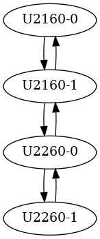
Due to this restrictive connectivity, there are cases where paging
thunks are linked to get from e.g. the primary U2160-0 bank to
a service function in e.g. U2260-0.
The second generation implementation is fully connected:
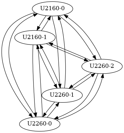
This is much more natural as it allows a single thunk to reach a service function in any bank.
The 2465B-late is Special
In the 2465B that have the SMD A5 board the memory map is very different than earlier generations. Rather than using 4/5 banks of 32/24k and overlaying one of them with the 8k RAM, all the banking is done in the last 16k of memory. This is all implemented by the very special Intel 8*16*8 paged EPROM chip, which latches the requested page on any write to the chip’s address space.
The late-B A5 board also subsumes the options buffer board as well as the A4 character generation board, though that’s neither here nor there in regards to banking. It’s just Very Special.